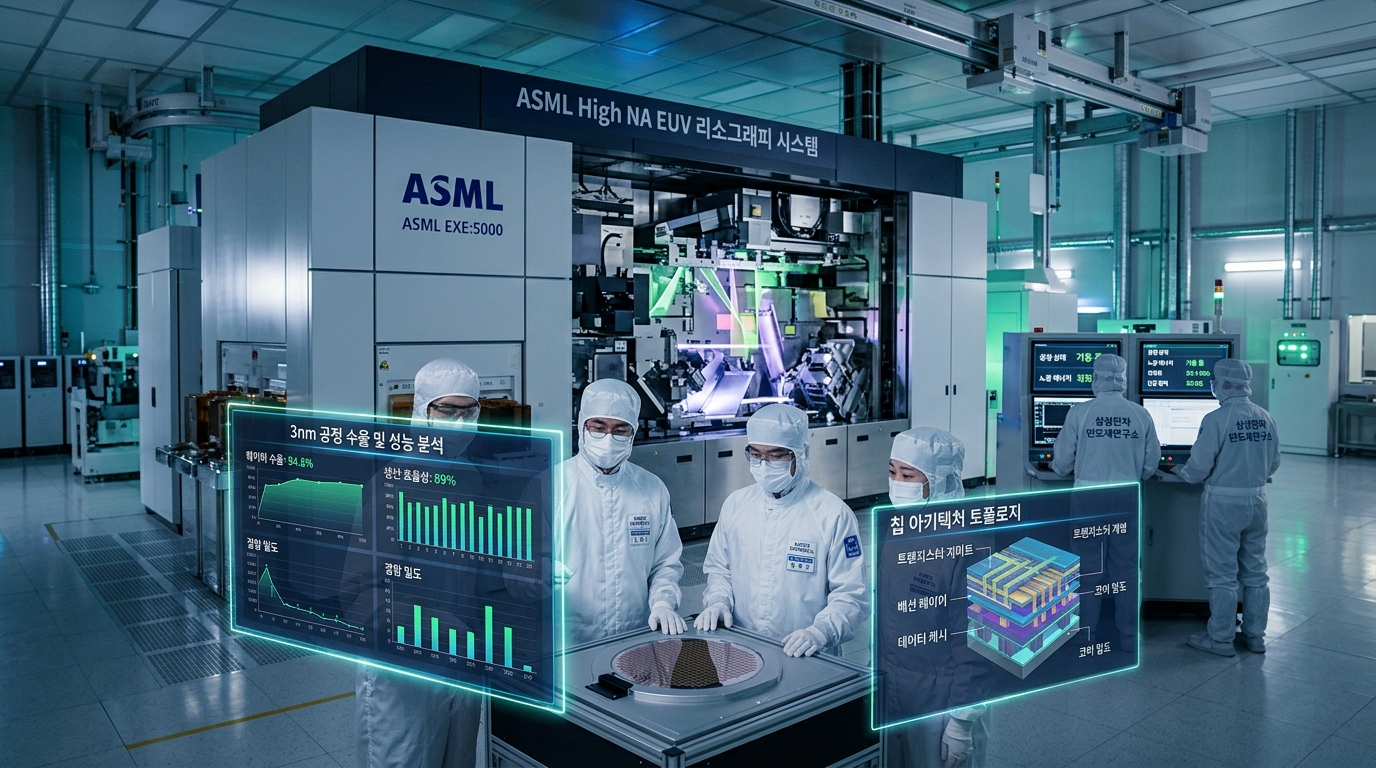
Market attention is focusing on ASML, the holder of the exclusive key to the global advanced semiconductor supply chain, as its High NA EUV (High Numerical Aperture Extreme Ultraviolet) backlog and foundry delivery schedules become increasingly visible.
[이미지: /stdaily/uploads/202609/gen_6ab5b9af2bb9a4.04251122.png]
Executive Summary
- **Monopolistic Equipment Dominance**: Second-generation High NA EUV systems (TWINSCAN EXE:5200B), priced at approximately $400 million (around 540 billion KRW) per unit, have officially entered the next-generation process roadmaps of the top three global foundries (Intel, TSMC, and Samsung Electronics).
- **Differentiated Foundry Delivery Timelines**: Following Intel's early adoption for 18A/14A, Samsung Electronics has formalized plans to deploy High NA for advanced DRAM mass production by 2028, while TSMC presented a roadmap targeting high-volume production by 2030 and pilot operation of a 12-inch photomask line by 2031.
- **Upward Revision of Guidance**: Backed by strong Q2 2026 results, ASML management raised full-year revenue guidance from the previous range of €36 billion–€40 billion to €43 billion–€45 billion.
- **Market Sentiment & Macro Indicators**: As of intraday trading on September 25, 2026 (provisional), the Nasdaq Composite stood at 26,939.37. Daily Stock's proprietary Fear & Greed Index registered 36.1 (Fear) for the Nasdaq and 53.8 (Neutral) for the KOSPI, reflecting cautious investor sentiment.
Current Situation Overview
Surging demand for AI accelerators and High Bandwidth Memory (HBM) is driving hyperscalers to expand infrastructure capital expenditures (CapEx), intensifying competition to secure advanced lithography systems.
In September 2026, ASML officially launched the "12-Inch (6×12-inch) Photomask Alliance" alongside Intel, TSMC, and Samsung Electronics to overcome High NA EUV exposure constraints, actively leading ecosystem standardization.
In terms of equipment delivery, Intel leads the pack after completing EXE:5200B acceptance testing primarily at its Oregon fab, amassing wafer processing data exceeding 1 million units.
Conversely, TSMC, prioritizing yield and cost-efficiency, is pursuing a more measured strategy—maximizing existing 0.33 NA Low NA EUV multi-patterning before transitioning to High NA mass production around 2030.
Memory powerhouse Samsung Electronics has decided on an early rollout of High NA EUV targeted for 2028 to advance DRAM scaling, aiming to regain next-generation process competitiveness.
[이미지: /stdaily/uploads/202609/gen_6ab5b9ba125c41.04130355.png]
Financial Analysis
ASML's financial stability stems from its monopolistic market position and a multi-year equipment order backlog.
According to Q2 2026 earnings, net sales reached €9.326 billion and net income stood at €2.918 billion, beating consensus estimates.
| Key Financial Metric | FY 2025 (Actual) | Q2 2026 (Confirmed) | FY 2026 Guidance (Revised Up) |
|---|---|---|---|
| **Net Sales** | €32.7 billion | €9.326 billion | €43.0 billion – €45.0 billion |
| **Gross Margin** | 52.8% | 54.0% | 54.0% – 56.0% |
| **Net Income** | €9.609 billion | €2.918 billion | Continued beat versus consensus |
| **Diluted EPS** | €24.73 | €7.59 | Consecutive quarterly gains |
| **Installed Base Management (Service) Revenue** | ~€8.6 billion | €2.762 billion | Double-digit annual growth maintained |
Backed by its robust backlog, ASML confirmed plans to expand its annual 0.33 Low NA EUV production capacity by 30% by 2027.
As higher-margin High NA equipment revenue is recognized progressively, gross margins are expected to remain solid around the 55% range.
Valuation
As of September 25, 2026, ASML's exact intraday quote remains unconfirmed (trading around €1,500–€1,600 based on recent updates), continuing to command a monopoly premium in the market.
Its 12-month forward P/E ratio trades in the mid-to-high 40s, hovering near the upper end of its historical mid-range.
Because its valuation multiples remain elevated compared to the Nasdaq 100 (NDX) index and S&P 500 large-cap growth stocks, its sensitivity to macroeconomic shifts is relatively high.
Compared to the Philadelphia Semiconductor Index (SOX), ASML benefits from a backlog structure that offers lower volatility and greater visibility than fabless chip designers, acting as a supportive factor for valuation.
However, a rebound in the US 10-year Treasury yield (US10Y) or sharp fluctuations in the US Dollar Index (DXY) could readily place multiple-compression pressure across high-growth tech stocks.
Expert & Institutional Analysis
Major Wall Street and European investment banks evaluate that High NA EUV entering commercialization has significantly improved ASML's medium-to-long-term revenue visibility.
Global brokerages, including Barclays, noted that the formal inclusion of High NA in TSMC's and Samsung's roadmaps has resolved market skepticism regarding equipment adoption delays.
Analysts emphasize that annual hyperscaler infrastructure spending has crossed $600 billion, keeping chipmakers' tool ordering within a structural expansion cycle.
On the other hand, some cautious observers point out that astronomical unit costs near $400 million and transition costs to 12-inch mask formats could burden foundry customers' CapEx efficiency.
There is also a view that the extent of deceleration in legacy DUV revenue due to export controls on China could interact with High NA revenue growth, potentially causing intermediate earnings volatility.
Risk Factors
The most direct risk is potential scaling back of semiconductor CapEx if Big Tech hyperscalers face delays in AI monetization.
If the monetization speed of AI software and services fails to keep pace with equipment investments, foundry customers may defer delivery schedules for High NA systems.
A second risk involves geopolitical and export control regulations.
As US and European restrictions on semiconductor equipment exports to China intensify, the share of legacy DUV tool shipments bound for China faces a gradual phase-down.
A third factor is monetary policy and receding rate-cut expectations.
If 10-year Treasury yield volatility widens or the Federal Reserve's pivot path falls short of market expectations, discount rates applied to high-multiple tech names will rise.
[이미지: /stdaily/uploads/202609/gen_6ab5b9c41c1f84.84685558.png]
Investment Perspective
Armed with an irreplaceable monopoly in extreme ultraviolet lithography, ASML commands a decisive bottleneck in the long-term AI paradigm.
As of intraday trading on September 25, 2026 (provisional), the KOSPI stood at 7,080.92, the KOSDAQ at 844.48, and the USD/KRW exchange rate was 1,366.70 KRW.
According to Daily Stock's proprietary Fear & Greed Index analysis, the Nasdaq index sits in Fear (36.1), improving slightly from Fear (28.3) a week ago, yet still contracted compared to Neutral (55.0) a month prior.
The KOSPI Fear & Greed Index sits at Neutral (53.8), rebounding from Fear (30.6) a week ago, though risk appetite has not fully recovered.
Therefore, investors should monitor near-term volatility gauges (VIX) and macro indicators, pacing investments alongside equipment delivery timetables and quarterly order backlog trends.
Investor Checkpoint Q&A
Q1. What technical advantages does High NA EUV offer over conventional Low NA EUV?
A1. High NA systems (0.55 NA) increase the lens numerical aperture to reduce single-exposure resolution down to 8 nm. This replaces complex multi-patterning processes with a single exposure, boosting chip density by approximately 2.9 times and substantially cutting process steps.
Q2. How do the High NA EUV deployment roadmaps differ among the top three foundries?
A2. Intel is adopting it earliest, conducting mass production trials for its 18A/14A nodes. Samsung Electronics has formalized DRAM deployment targeting 2028, while TSMC has signaled a measured approach with mass production around 2030 and a 12-inch mask line by 2031.
Q3. What drove ASML's upward revision to its 2026 full-year guidance?
A3. Tool orders accelerated from chipmakers responding to surging demand for AI accelerators and HBM. Management consequently raised full-year 2026 revenue guidance from €36B–€40B to €43B–€45B.
Q4. What is the significance of the recently announced "12-Inch Photomask Alliance"?
A4. Because High NA tools utilize anamorphic optics that halve the exposure field, stitching constraints arise when producing large-die AI chips. To resolve this, the alliance seeks to co-develop a 12-inch photomask standard replacing the current 6-inch format, maximizing mass production efficiency.
Q5. What macro and fundamental variables should investors watch most closely?
A5. Trends in the US 10-year Treasury yield (US10Y) and quarterly AI infrastructure CapEx execution rates from Big Tech hyperscalers. Investors must also track US-China export restriction developments on chip equipment and broader VIX volatility dynamics.