Hello, this is Daily Stock, delivering the core pulse of the Nasdaq and global tech industries.
[이미지: /stdaily/uploads/202610/gen_6ac9803c957cf9.71421494.png]
Key Summary
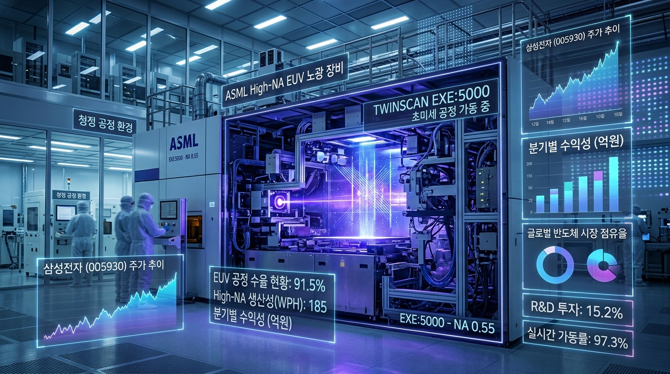
The commercialization cycle for next-generation High-NA EUV lithography systems (numerical aperture 0.55) has officially entered the phase of volume mass production tool deliveries and foundry integration. Priced at roughly $400 million per unit, the High-NA EUV system is regarded as the definitive technological weapon dictating yield and productivity in sub-2nm and 1.4nm-class advanced fabrication nodes.
While Intel has taken the most aggressive stance by adopting the initial evaluation tool EXE:5000 followed by the mass production EXE:5200 series, TSMC and Samsung Electronics are also ramping up their competitive bids, participating in the next-generation large-scale photomask alliance and mapping out High-NA deployment. Amid high interest rates and Big Tech CAPEX cycles, ASML's delivery pace serves as a primary benchmark determining valuation multiples across the global semiconductor value chain.
Current Situation Summary
As of October 10, 2026, global financial markets continue a fierce tug-of-war between macroeconomic volatility and the sustainability of AI hardware capital expenditures (CAPEX). The Nasdaq index stands around 27,366.17, the USD/KRW exchange rate closed at 1,342.00 KRW, KOSPI closed at 6,625.93, and KOSDAQ ended at 892.27.
Looking at Daily Stock's proprietary sentiment indicators, the Nasdaq Fear & Greed Index currently sits at 'Neutral (45)', shifting toward a gradual wait-and-see posture away from trough fear levels compared to 1 week ago (Fear, 40), 1 month ago (Fear, 38.2), and 3 months ago (Neutral, 48.6). Conversely, the KOSPI Fear & Greed Index is at 'Fear (24.4)', showing contracted sentiment compared to 1 week ago (Neutral, 40.1) and 1 month ago (Neutral, 50.9).
While the intraday share price of ASML (ASML) remains unconfirmed (based on the latest verified metrics), the delivery velocity of High-NA EUV tools and the fab accommodation timelines of major foundries are driving sentiment across the broader semiconductor sector. As volume manufacturing schedules (EXE:5200B) materialize beyond initial R&D supply phases, cost-benefit calculations weighing steep tool acquisition prices against process efficiency gains have begun in earnest.
[이미지: /stdaily/uploads/202610/gen_6ac98047876bd6.94187218.png]
Financial Analysis
ASML's mid- to long-term earnings visibility directly hinges on its ability to execute its substantial backlog of high-ASP EUV and next-generation High-NA systems. Costing between $350 million and $400 million per unit, High-NA EUV systems carry a price tag nearly double that of legacy Low-NA NXE tools, serving as a critical pillar to defend gross margins in the mid-to-high 50% range.
| Classification | Low-NA EUV (NXE Series) | High-NA EUV (EXE Series: 5000 / 5200B) |
|---|---|---|
| **Optical Numerical Aperture (NA)** | 0.33 | 0.55 |
| **Single Exposure Resolution** | ~13nm | ~8nm (2.9x transistor density improvement effect) |
| **Estimated Tool Price** | ~$180M – $220M | ~$380M – $400M+ |
| **Wafers Per Hour (WPH)** | ~160 – 220 WPH | EXE:5000 (Early), EXE:5200B (Targeting 175+ WPH) |
| **Major Customer Roadmap** | All global leading-edge foundries & DRAM mass production | Intel (14A, etc.), Samsung Electronics (DRAM/leading-edge nodes), TSMC (A14/A10 class) |
Despite the heavy depreciation burden placed on foundries, High-NA adoption is pursued because replacing double- or triple-patterning steps with a single exposure reduces process complexity and lowers defect rates. As tool delivery revenues are progressively recognized in quarterly financial results, ASML's cash flow generation and capacity for shareholder returns (share buybacks and dividends) are positioned for stepwise expansion.
Valuation
Within the Nasdaq 100 and the Philadelphia Semiconductor Index (SOX), ASML has sustained a notable valuation premium over the S&P 500 growth average, anchored by its irreplaceable monopoly position. Its forward price-to-earnings (Forward P/E) ratio has historically maintained a band between the mid-30s and low-40s, a reflection of the safety margin afforded by its sole-source lithography ecosystem.
However, elevated 10-year US Treasury yields (US10Y) and a resilient US Dollar Index (DXY) act as macroeconomic headwinds capping broad valuation re-ratings for high-multiple tech names. As risk-free discount rates rise, the present value of future free cash flows (FCF) generated from long-tail tool deliveries faces compression.
Concurrently, whenever market volatility spikes via the VIX, ASML faces vulnerabilities as concerns over tool delivery delays or client CAPEX retrenchment are rapidly priced in. For current valuation premiums to remain justified, foundries must demonstrate actual fab deployment and follow-through repeat orders for volume production.
Expert and Institutional Analysis
Wall Street and global semiconductor research institutions are closely tracking the divergent strategies among the top three foundries regarding High-NA EUV adoption. Intel Foundry has aggressively onboarded High-NA equipment early on to validate its 18A process and accelerate commercialization of its next-generation 14A node in a bid to surpass rivals.
Conversely, market leader TSMC is taking a more conservative approach, maximizing its established patterning expertise on existing Low-NA EUV tools to optimize cost-to-yield efficiency before deploying High-NA into volume manufacturing around 2030 for its ultra-advanced nodes. Samsung Electronics is targeting synergies across both advanced foundry nodes and next-generation memory scaling, having formalized plans to incorporate High-NA into volume DRAM lines by 2028.
Institutional analysts view the recent agreement between ASML and the three major chipmakers to build a 12-inch next-generation photomask ecosystem as a structural tailwind. By outlining a roadmap to overcome the exposure field size constraint (stitching issues) caused by traditional 6-inch mask standards, the industry has laid the groundwork to reduce mass production costs for massive AI accelerator chips by roughly 40%.
Risk Factors
The most fundamental risk centers on potential delays in Big Tech's return on investment (ROI) from AI infrastructure. If hyperscaler data center CAPEX continues to outpace the pace of generative AI monetization, foundries may postpone capacity expansions for advanced nodes, delaying High-NA tool delivery schedules.
Second is the macro discount rate burden stemming from prolonged higher interest rates. Should volatility in the 10-year US Treasury yield (US10Y) widen or the US Dollar Index (DXY) surge, high-multiple growth equities characterized by multi-year tool manufacturing cycles could face severe multiple compression.
Third is geopolitical friction and stringent export controls targeting China. As Dutch authorities and the US Department of Commerce maintain or expand restrictions on advanced lithography shipments, performance volatility could intensify if Western foundry High-NA orders fail to fully compensate for lost demand in trailing-edge DUV tools.
Investment Perspective Summary
Evaluating ASML requires looking beyond raw unit shipment figures to adopt a scenario-based approach focused on client foundries' execution of next-generation process roadmaps. High-NA EUV remains the sole path forward to overcome physical semiconductor scaling limits, yet it presupposes robust AI chip demand capable of offsetting massive fab retrofitting costs and astronomical equipment pricing.
With the Nasdaq Fear & Greed Index currently lingering in 'Neutral (45)' territory, this environment calls for a sober assessment of long-term fundamentals rather than reacting to technical overheating or capitulation selling. A disciplined approach requires cross-referencing ASML's relative strength against the SOX index, stabilization trends in 10-year US Treasury yields, and changes in 2026–2027 CAPEX guidance from TSMC, Intel, and Samsung Electronics.
[이미지: /stdaily/uploads/202610/gen_6ac98052853817.31998844.png]
Q&A with Daily Stock
Q1. What is the core technical difference between High-NA EUV and legacy EUV systems?
A1. The primary distinction lies in boosting the numerical aperture (NA) of the optical projection lens from 0.33 to 0.55. Without altering the light source wavelength, this refines single-exposure resolution from approximately 13nm to 8nm, eliminating multiple patterning steps and decreasing defect densities in sub-2nm processes.
Q2. Why do Intel, TSMC, and Samsung Electronics have differing High-NA adoption timelines?
A2. Their roadmaps reflect differing process strategies and cost structures. Intel aims for early mass deployment (e.g., 14A) to seize foundry leadership, whereas TSMC intends to extract maximum economic efficiency from Low-NA systems before transitioning to High-NA around 2030. Samsung Electronics has officially scheduled adoption for next-generation DRAM mass production by 2028.
Q3. Is the near-$400 million price tag per tool overly burdensome for foundries?
A3. The upfront CAPEX and subsequent depreciation expenses are substantial. However, by replacing complex multi-patterning passes with a single exposure, the technology can lower per-die manufacturing costs over the long run once production yields and target wafer throughput are fully validated.
Q4. Why is the recent move toward a 12-inch next-generation photomask standard significant?
A4. Due to the anamorphic lens design in High-NA optics, the exposure field is halved, requiring die stitching when printing large AI accelerator chips. Standardizing and co-developing a 12-inch photomask rather than conventional 6-inch reticles eliminates this bottleneck, significantly improving manufacturing efficiency.
Q5. Why do fluctuations in 10-year US Treasury yields matter for ASML investors?
A5. ASML trades as a premium, high-multiple equipment stock whose valuation heavily discounts long-term future growth. Rising Treasury yields increase discount rates applied to future cash flows, compressing valuation multiples (P/E), while also raising debt financing costs for chipmakers, which can slow down fab CAPEX deployment.